 Tiny Online Tools

Gerber PCB Viewer: The Fastest Way to Inspect PCB Layers
Gerber PCB Viewer: The Fastest Way to Inspect PCB Layers
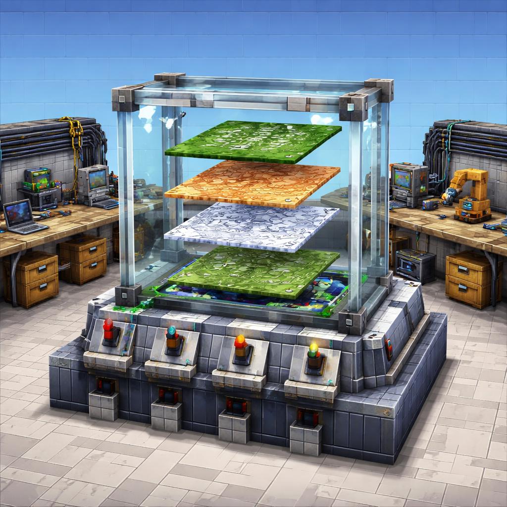
If you’ve ever opened a Gerber package and felt like you were staring at a pile of mystery files, you’re not alone. PCB fabrication files can be precise, powerful, and a little intimidating. That’s exactly why Gerber PCB Viewer matters: it helps you overlay a Gerber/Excellon fabrication package as a realistic PCB image, with copper, soldermask, silkscreen, and drill layers toggled on or off.
That simple workflow can save time, catch mistakes early, and make a design easier to review with teammates, vendors, or clients. Whether you’re checking a prototype before fabrication or just trying to understand what’s inside a board package, Gerber PCB Viewer gives you a fast visual read on the final board.

Why a Gerber viewer is worth using
Gerber files are the standard language of PCB fabrication, but the raw files themselves are not very human-friendly. A good Gerber viewer translates those layers into something you can inspect visually.
With this tool, the big win is context. Instead of mentally reconstructing a board from separate outputs, you can see how the copper, mask, silkscreen, and drill information align. That makes it easier to spot missing details, misaligned drill holes, or a board outline that doesn’t look quite right.
Common use cases
Here are a few situations where Gerber PCB Viewer is especially handy:
- Pre-fab sanity checks — quickly verify the board looks like the design you intended before sending it out.
- Client or teammate reviews — show a realistic PCB image instead of asking someone to interpret individual layer files.
- Manufacturing handoff — inspect how copper, soldermask, silkscreen, and drills line up before release.
- Troubleshooting surprises — when a board comes back wrong, compare the fabrication package visually to understand what may have gone off track.

How to use it
You don’t need a complicated workflow to get value from a PCB viewer. A quick pass is often enough.
Step 1: Open the tool
Go to Gerber PCB Viewer and load your fabrication package.
Step 2: Inspect the layers
Toggle the layers you care about most: copper, soldermask, silkscreen, and drill data. Look for alignment, missing features, and anything that looks visually off.
Step 3: Review the overall board image
Once the layers are visible together, check whether the board “reads” correctly as a complete design. This is often the fastest way to catch issues before fabrication.
Step 4: Re-check problem areas
If something looks odd, isolate the related layers and inspect them again. Narrowing the view often reveals whether the issue is in the outline, the holes, or one of the artwork layers.
Tips for better reviews
A few habits make PCB inspection more effective:
- Start with the board outline. If the outline is wrong, everything else becomes harder to trust.
- Check drill placement against pads. Misplaced drills are easy to miss in raw data.
- Compare silkscreen to copper. Text and component markers should not overlap important features.
- Use a second pass after changes. Small edits can introduce new issues, especially late in the design cycle.

Related tools to know about
If you’re working around the same workflow, these tools are worth bookmarking:
- Gerber Preflight Checker for catching missing layers, an unclosed board outline, drills outside the board, and other common fab problems.
- Gerber to SVG/PDF for turning Gerber/Excellon layers into a scalable SVG or a PDF sized to the board’s physical dimensions.
- DXF Layer Viewer for opening a DXF drawing in the browser and toggling layers on or off.
- Universal CAD Viewer if you also need to inspect STEP, IGES, BREP, STL, or DXF files.
- CAD Viewer for browser-based viewing of STEP, STP, IGES, IGS, and BREP files.
When this tool shines most
The best time to use a PCB viewer is before fabrication, not after. It’s a small habit that can prevent expensive rework. But it’s also useful any time you need to explain a board layout to someone who doesn’t live in CAD tools all day.
For teams, the visual approach reduces confusion. For solo builders, it provides a much quicker confidence check than digging through every output file manually. And for fast-moving projects, that speed matters.
Final take
If you regularly deal with PCB fabrication files, a visual layer inspector is one of the simplest ways to reduce surprises. Gerber PCB Viewer helps you see the board the way manufacturing will see it, which makes review faster and more reliable.
Open it, inspect the layers, and give your next board a visual pass before it leaves your desk.